

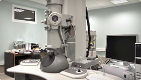


Transmission electron microscopy (Tecnai G2 F20 U-TWIN)
Scanning electron microscopy analysis types:
- Image acquisition of nanoscale objects (conductive and non-conductive) by methods of TEM, such as:
- nanoparticles (nanopowders),
- nanorods,
- nanofibers,
- nanotubes,
- nanowires,
- nanodisks
- Image analysis obtaining quantitative data about the size and shape of nano-objects, and the degree of agglomerable.
- Image acquisition by the TEM method of the sample structure of nanostructured materials with the spatial resolution down to 0.2 nm.
- Obtaining the surface stereoscopic topography images.
- Image analysis to afford quantitative data about the size and shape of the nanocrystals (granules), long intercrystallite boundaries and other features of the structure.
- Preparation by the TEM method pictures of cross section structures and sample surfaces of nanostructured thin object (conductive or nonconductive), including thin films, coatings, nanochips electrolyte and electrode structures with a spatial resolution down to 0.2 nm.
- Obtaining of the numerical data on the size of layers, the size and shape of the nanocrystals (granules), pores, intercrystallite boundaries, inter-layer interfaces and other features of the structure.
- Analysis of chemical elements distribution in the object (based on X-ray analysis).
- Investigation of point and line defects in materials - vacancies and dislocations.
- Potential distribution analysis of the complicated microproducts (Volts contrast).
- Investigation of magnetic field distribution in the sample (magnetic contrast).
- Microproducts metrology.

